

01
Expertise
Industry-seasoned instructors
Learn from experienced instructors. Build practical and theoretical skills aligned with current industry knowledge and standards.
Explore Expertise
Specialized VLSI Training
Start your VLSI career with training designed and delivered by industry experts. Learn practical skills through our Physical Design and Design Verification programs.



Choose a program that matches your career goals and gain hands-on experience with industry-standard tools and expert guidance.
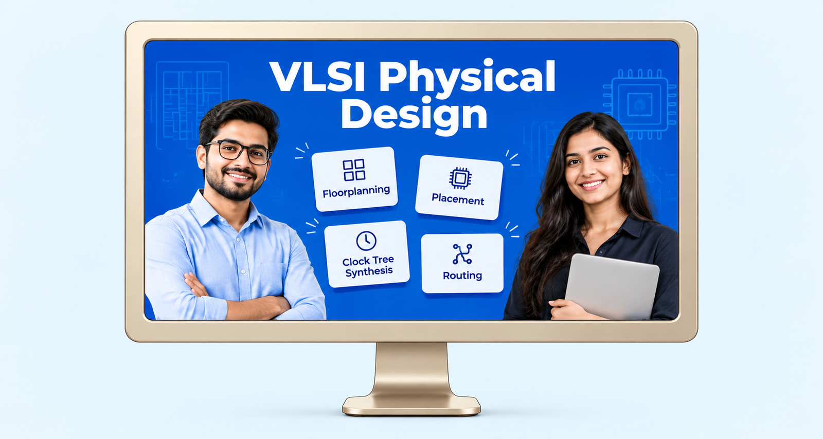
COURSE 1 OF 2
Study the complete physical design journey, from design preparation through implementation and sign-off.
What We Offer
A complete learning journey with expert guidance, practical exposure and career support to help you build a career in the semiconductor industry.
Learn from experienced instructors. Build practical and theoretical skills aligned with current industry knowledge and standards.
Explore ExpertiseStrengthen hands-on skills through practical industry projects, expert-led learning and professional connections.
Explore Internships
Receive hands-on training, personalized career and resume support, and placement opportunities with alumni support.
Explore Placement
Insights on VLSI design, semiconductor technology and career paths.
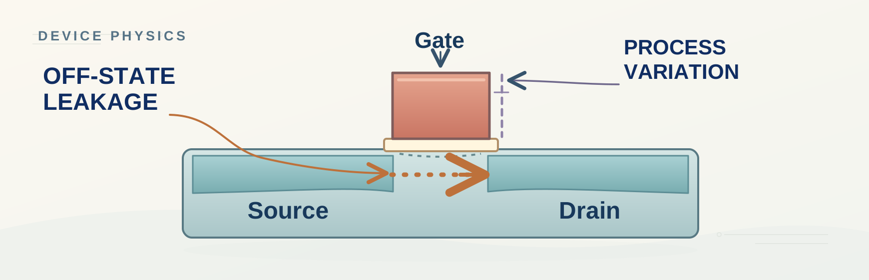
Explore challenges in power, performance and scaling. Learn how leakage, short-channel effects and process variation complicate advanced nodes, and why simulation and balanced PPA decisions matter.
Read Article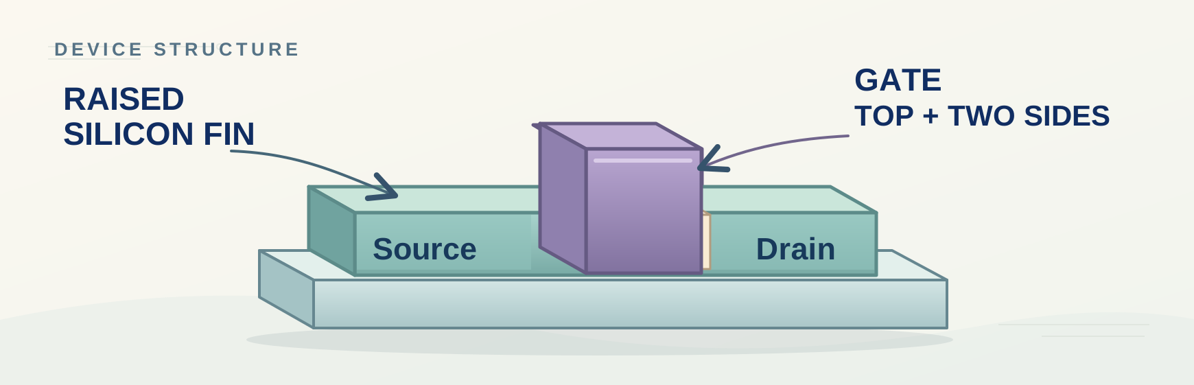
How FinFET transistors enable smaller and more efficient chips. See how a fin-shaped channel improves gate control, reduces leakage and short-channel effects, and changes implementation trade-offs.
Read Article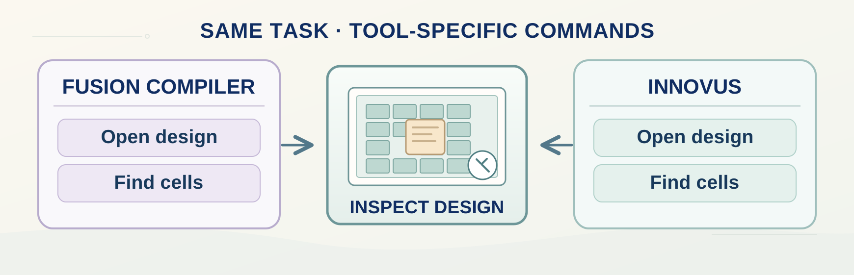
Compare Fusion Compiler and Innovus commands. This side-by-side mapping covers launching tools, opening designs, multi-CPU settings, design checks and timing checks to help you move between the two workflows.
Read Article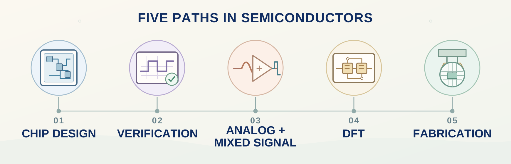
Explore chip design, verification and fabrication career paths. The article also covers analog and mixed-signal design and DFT, with the practical skills and tools needed to enter each role.
Read Article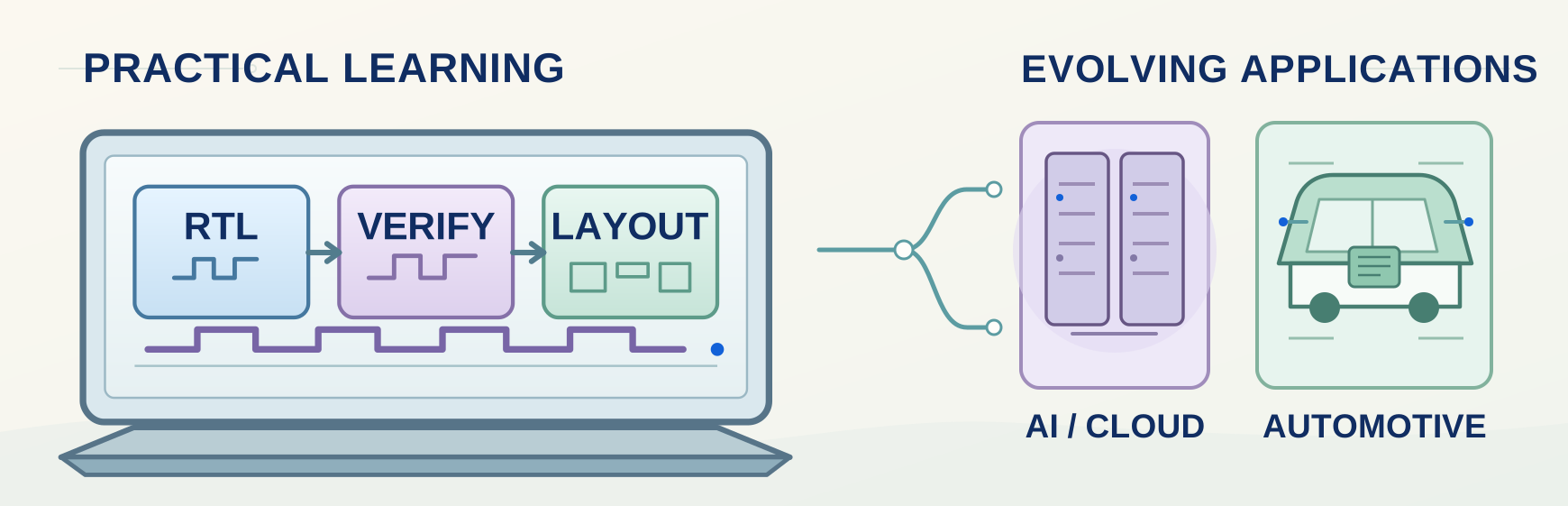
What engineering students can learn for a career in VLSI. Explore how chips now power AI, electric vehicles and connected products, and why projects, internships and continual upskilling matter.
Read Article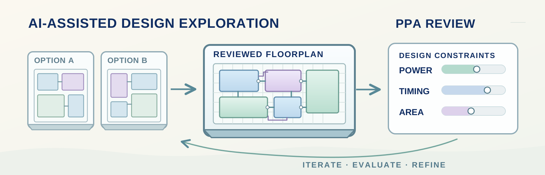
Explore six trends shaping electronics engineering, from AI and 5G to sustainable and quantum technologies. See how smaller nodes and new design approaches are changing the skills VLSI engineers need.
Read Article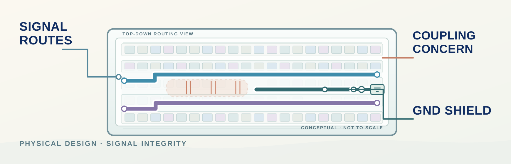
Understand process variation, leakage, signal integrity and tool challenges at advanced nodes. Learn how power gating, routing, shielding and specialized EDA methods help address sub-10nm constraints.
Read ArticleExplore challenges in power, performance and scaling. Learn how leakage, short-channel effects and process variation complicate advanced nodes, and why simulation and balanced PPA decisions matter.
Read Article“The Abhyasa courses have transformed my understanding of VLSI. The trainers are very supportive!”
 Rajesh
“An amazing platform for VLSI training. The blend of online and offline classes is perfect.”
 Narendra
“I learned so much from Abhyasa's in-depth courses. Highly recommend it for aspiring engineers!”
 Shekar
Share your details and our team can help you get started.
We are here to help with course details, admissions and any queries.
Call us for any queries
+91 9438062982Drop us an email
abhyasasemitech@gmail.comhr@abhyasa.org.inVisit our institute
2nd Floor, Akhila Arcade, Rama Talkies Road, Asilmetta Junction, Visakhapatnam – 530016, Andhra Pradesh, India.